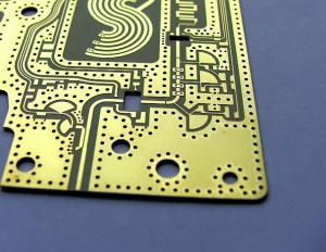
At Pure PCB the development of our PCB Technology means much more to us than just a desired state of affairs on a technology road map; it means putting our customers current and future requirements at the forefront of all our development activities.
 Our focus on creating high mix low volume manufacturing capacity allows us space and resources to provide a testing ground for our customer needs, be it trialling new material systems, creating complex HDI designs, or providing solutions to thermal management challenges.
Our Customer Technology team work directly with our customer to define their technology needs outside of their day to day operational PCB needs, and establish the right fit long term strategy to support.
This strategy may address gaps between current capability and the development need of the PCB, or may optimise the current manufacturing capability to support the product requirement.

Intelligent Innovation.
At Pure PCB we operate under the basic premise that the innovations we bring to bear need to add near term benefits and provide intelligent solutions to real word problems.
Across our manufacturing capability we have implemented a process called "Intelligent Innovation" which alows us to reconcile conversations we have with customers right from the earliest stages of their designs, allowing us to conduct an ongoing dialogue in regard to our ability to support the design need. By assesing our capability at the earliest stages of the design conversation, we are able to challenge ourselves and our manufacturing to provide the "Intelligent Innovations" at the right time, and at the right cost point - for more information on our "Intelligent innovation" process please see the detail below.
Recent examples of where Pure PCB have provided technology solutions to some of our customer challenges
- Developing a robotic handling system to improve the handling and touch time for thin cores.
- Implementing a warp and weft reference frame to ensure correct orientation of RF laminate for a small antenna PCB.
- Implementing a high copper weight solution for a customer demand and working through to UL approval.
- Developing a secure test and serialisation solution for a fragile mission critical flex circuit, giving the customer a known good circuit prior to assembly.
