HDI PCB Manufacturer
Pure PCB's HDI PCB Technology (High Density Interconnect) is one of the many PCB Capabilities we possess and enables PCB designers to create increasingly complex designs, with optimal layout formats, across a wide range of technologies. Offering 4 through to 28 layers, our HDI PCB’s are available in various thickness – from 0.3mm to 3.5mm, with a minimum line width and space from 0.075mm. Learn more about Pure as HDI PCB suppliers, as well as the different options of HDI printed circuit boards as we have available.
What is HDI PCB?
HDI PCBs are printed circuit boards which use HDI technology – a technology which enables a compact yet reliable PCB design. HDI PCBs typically have smaller vias and capture pads, finer lines and spaces and a higher connection pad density, than conventional PCB technology.
At Pure PCB, our HDI PCBs allow increased flexibility - by combining fine track and gap features along with laser-drilled blind or buried Microvia Technology, this allows interconnection of one PCB layer to another using the smallest pad diameter possible. This, in turn, allows greater flexibility of HDI printed circuit board design through increased real estate utilisation on the circuit.
Types of HDI PCBs
As a leading HDI PCB supplier, we supply various types and sizes of high-density interconnect PCBs. With via sizes of typically =< 150µm, with a pad diameter requirement of typically =< 300µm, Pure PCB offers a full suite of Microvia Technology from single through to stacked microvia, via epoxy filled and copper plating including solid copper fill and plated shut circuits.
- Suitable HDI surface finishes: ENIG, Lead Free HASL, Immersion Silver, Immersion Tin, OSP, ASIG, ISIG.
- Suitable HDI Materials available: Standard TG FR4, High TG FR4, Taconic, Rogers, Arlon, Nelco, Isola, Halogen free FR4.
- Via fill options: Resin Fill via, Copper plated shut up to max 6L, Solder mask ink.
For more information on our HDI printed circuit boards, get in touch with a member of our expert team.
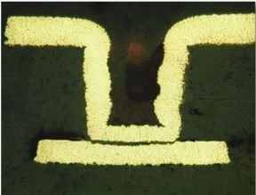
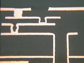
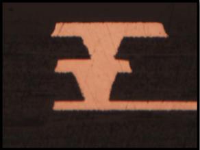
See below examples of Pure Electronics Microvia Solutions:
|
PCB |
Pure PCB Current Capability |
|
Available HDI Technology |
2-24 Layers |
|
1+N 1 |
|
|
2+N+2 |
|
|
3+N+3 |
|
|
4+N+4 |
|
|
Full Layer Interconnect Available |
|
|
Available PCB Thickness |
0.3 mm to 3.5 |
|
Minimum Line Width and Space |
From 0.075mm |
|
Available Suitable HDI Surface Finishes |
ENIG |
|
Lead Free HASL |
|
|
Immersion Silver |
|
|
Immersion Tin |
|
|
OSP |
|
|
ASIG/ISIG |
|
|
Suitable HDI Materials Available |
Standard TG FR4 |
|
High TG FR4 |
|
|
Taconic/Rogers/Arlon/Nelco/Isola |
|
|
Halogen Free FR4 |
|
|
Minimum Available Drill Size |
Mechanically Drilled 0.15 |
|
Laser Drilled 0.1mm |
|
|
Aspect Ration 1:0.8 |
|
|
Via Fill Option |
Resin Fill Via |
|
Copper plated shut – up to max 6L |
|
|
Solder Mask Ink |
 Single Microvia
 Blind & Buried Microvia

Stacked Microvia
