
Secure Front End Engineering
Pure PCB believe that managing your PCB production securely and effectively starts at the front end engineering process. We offer unparalleled security in our front end engineering, working closely with suppliers and you to ensure the highest quality.
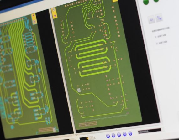
Our UK and Manila based Front End Engineering teams using CAM350 & Genesis 2000 CAM systems ensure that our customers designs are fully compliant and compatible with our PCB production process. Quality assurance is also vital when creating PCBs – to ensure that key error detection checks are taken and corrective actions are implemented we work in conjunction with the customer and our expert team.
Our PCB Checks
All of our New PCB production are run through a series of key stages prior to board panelisation.
- Checking of Minimum Air Gap
- Open Trace Checks
- Power to Ground Short Detection
- Annular Ring Verification
- Exposed Trace Review
- Fab to Gerber Misalignment.
- Minimum Trace Review
In addition to these design rule checks we also review the data for optimisation to ensure maximum efficiency in production – these include:
- Netlist Compare
- Line Unification
- Redundant Line Removal
- NFP Removal
- Pad Registration checking
- Exposed Copper Detection
- Solder Mask Creation
- Signal Layer Optimisation
- Line Width Optimisation
- Power & Ground Optimisation
- Copper Balancing
- Etching Compensation
Having concluded the PCB front end engineering process, a PCB tooling kit is generated containing full details for manufacture. This includes a stepped solder paste mask for SMT Screen Generation - a copy of which is provided to the customer as part of First Article Inspection PCB verification process.
Interested in working with a PCB manufacturer that values secure front end engineering and high quality production? Get in touch with a member of our friendly sales team today!